Dissecting Raspberry Pi Embedded Java Hello World
Overview
My prior posts1 showed how to build and deploy an embedded Java hello world application on a Raspberry Pi Zero. In this post, I will dissect the hello world program itself to give you some insight into how Java, the HaikuVM project, and hardware datasheets combine to produce working embedded Java applications on the Raspberry Pi.
It is important to understand that in true bare-metal embedded programming (which to me means no operating system), you interact with hardware directly. My attraction to this world is that all the abstraction is stripped away. You are forced to reconcile how software and hardware work together. I still want to use high-level language constructs, but I want to talk to the hardware directly for performance, dependability, size, or even legal reasons.
Know Your Goal
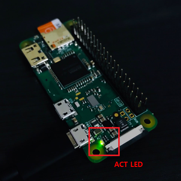
Our goal is to make the green ACT LED on the board blink. Where do we start?
Knowing What To Do And Knowing How To Know
Importance Of Schematics and Datasheets
So how do you know how to interact with the hardware directly? Enter the world of schematics and hardware datasheets. If as a new software developer, or perhaps an experienced engineer mainly working on business systems, you have never looked at a datasheet, prepare to have mind blown. These monstrosities are hundreds and sometimes thousands of pages.
You do not have to read it all! But you do have to read the important parts. Let’s use the Raspberry Pi Zero as a test case.
Use Your Map
When a journey is first planned, a map is usually handy. In this case, a schematic diagram is our map. The Raspberry Pi foundation is a good place to start.
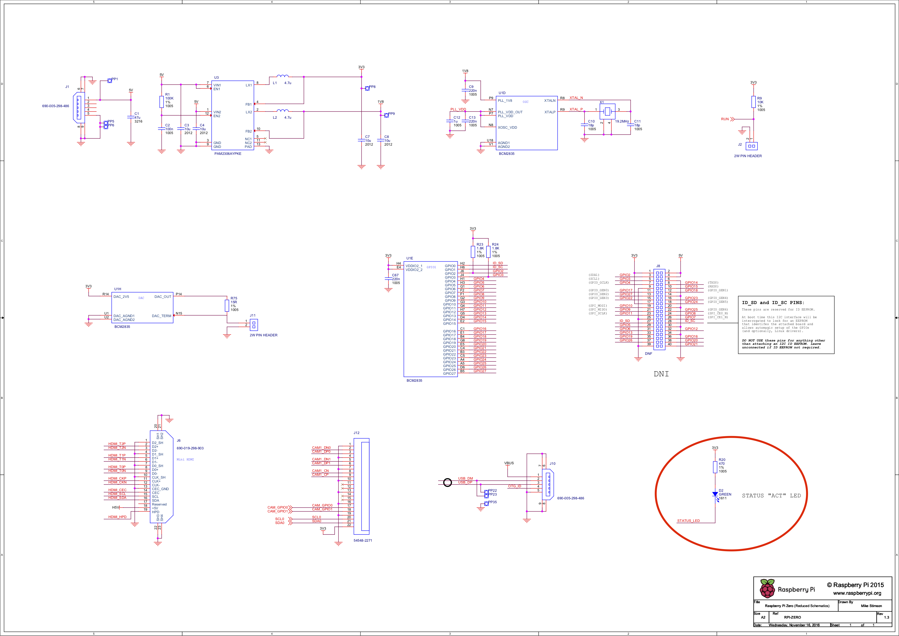
I have circled the LED. You can see the anode (the triangle symbol) is connected to +3.3v and the cathode (the line symbol) is connected to STATUS_LED. To make the LED light, you need a voltage potential between the two points, which means that STATUS_LED must be driven down to 0v. So how do we manipulate STATUS_LED? If you look carefully, you will notice that the tag has no corresponding label terminating it to another device. This is a documentation error2. What to do?
Rely On The Work Of Others
Cheat. Because Linux can run on the Raspberry Pi, I find that the device tree source code is very useful. This trick works for any hardware that runs Linux. In the Pi Zero case, we see:
/*
 * Copyright (C) 2016 Stefan Wahren <stefan.wahren@i2se.com>
 *
 * The code contained herein is licensed under the GNU General Public
 * License. You may obtain a copy of the GNU General Public License
 * Version 2 or later at the following locations:
 *
 * http://www.opensource.org/licenses/gpl-license.html
 * http://www.gnu.org/copyleft/gpl.html
 */

/dts-v1/;
#include "bcm2835.dtsi"
#include "bcm2835-rpi.dtsi"
#include "bcm283x-rpi-usb-host.dtsi"

/ {
	compatible = "raspberrypi,model-zero", "brcm,bcm2835";
	model = "Raspberry Pi Zero";

	leds {
		act {
			gpios = <&gpio 47 GPIO_ACTIVE_HIGH>;
		};
	};
};

&gpio {
	pinctrl-0 = <&gpioout &alt0 &i2s_alt0 &alt3>;

	/* I2S interface */
	i2s_alt0: i2s_alt0 {
		brcm,pins = <18 19 20 21>;
		brcm,function = <BCM2835_FSEL_ALT0>;
	};
};

&hdmi {
	hpd-gpios = <&gpio 46 GPIO_ACTIVE_LOW>;
};
Notice under leds, the act LED says gpio 47. GPIO means “general purpose input output”. And this makes sense because this is a generic way to turn a voltage on or off, and that is all we have to do to get the LED to light. The top of the LED (called the anode) is directly connected to +3.3v. If we pull the bottom of the LED to ground (called the cathode and labeled STATUS_LED), the LED will light. How did Mr. Stefan Wahren find where STATUS_LED is connected so that he could write this code? Who knows. He probably asked the schematic author. “Oops, my bad, yeah, it’s pin 47” was probably how it went.
The Datasheet
So how do we find out how to twiddle GPIO 47? If you look back on the schematic, you can see that all the GPIO terminate into a block labeled BCM2835. A quick googling reveals that the BCM2835 is the Broadcom BCM2835 System on Chip (SoC). A bit more googling reveals the datasheet for BCM2835 peripherals, our first 205 page document! You don’t have to read it all, or really much of it.
GPIO Registers
Searching in this document for for GPIO will lead you to page 89. There is a nice block diagram that is worth a careful look:
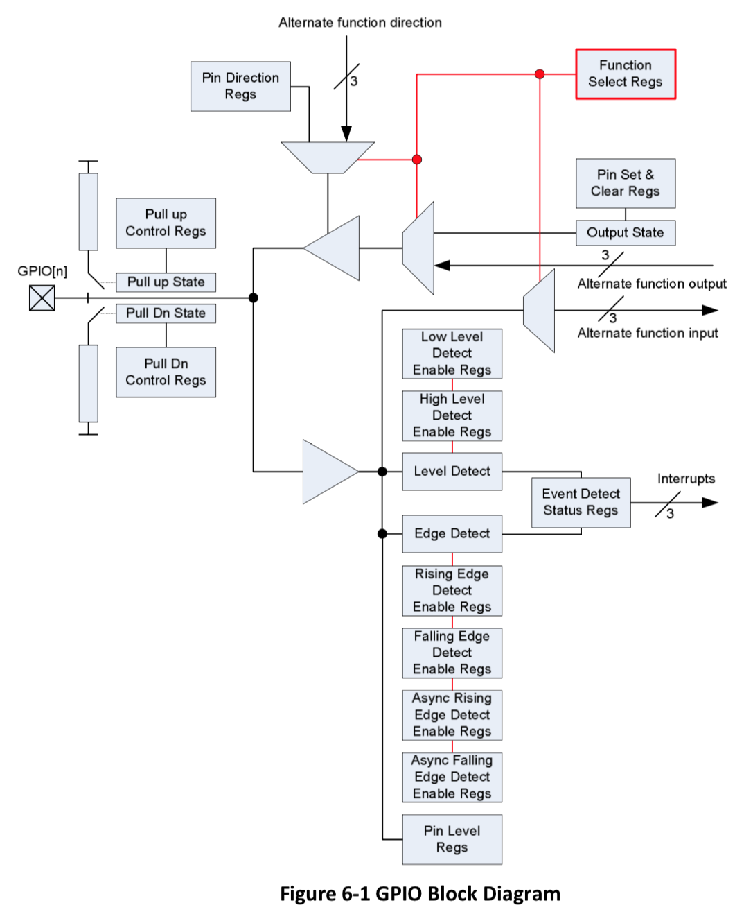
First, note the GPIO[n] square box with an X in it. It represents the set of pins on the device, one of which we are trying to twiddle. Second, “regs” are registers and registers are just memory locations, from a programming perspective. Third, the box in red Function Select Regs looks important because it implies these GPIO pins can perform multiple functions. That makes sense because as a GPIO, it can assert an output or take in an input. It’s in the name. Note the box Pin Direction Regs. The final box of interest is the Pin Set & Clear Regs. Setting and clearing a GPIO pin is what we are trying to achieve. So in review, to make the act LED flash, we will need to:
- Set the function select register for GPIO 47 to “output”.
- Loop forever
- Manipulate the GPIO 47 set register.
- Wait a bit
- Manipulate the GPIO 47 clear register.
- Wait some more.
So, what memory locations (registers) do we need to manipulate?
Setting A GPIO As Output
First look at the 6 (0 through 5) function selection register(s) on page 90:
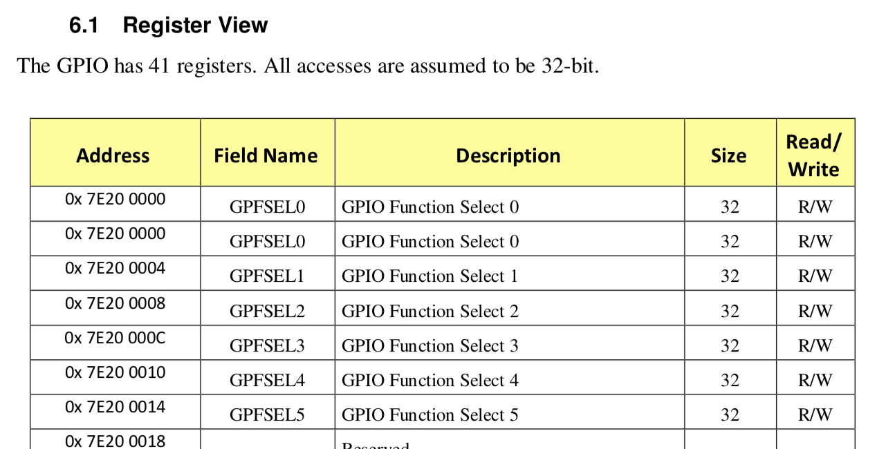
Note that each register (think memory location, labeled GPFSELn, and note they have addresses) is 32-bits in length. Why are there 6 of them? From the datasheet:
The function select registers are used to define the operation of the general-purpose I/O pins. Each of the 54 GPIO pins has at least two alternative functions as defined in section 16.2. The FSEL{n} field determines the functionality of the nth GPIO pin. All unused alternative function lines are tied to ground and will output a “0” if selected. All pins reset to normal GPIO input operation.
FSEL{n} fields define the function for the nth GPIO pin. And given that there are 54 pins, and registers are 32 bits long, it would stand to reason there there would have to be more than one function select register. So what do these FSEL fields look like and which register contains the FSEL for GPIO47?
If you look at pages 91-94, you’ll see tables like this:
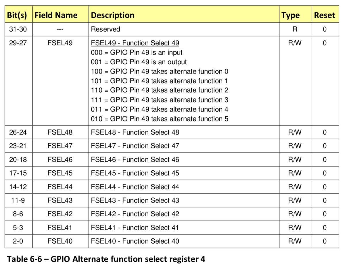
I happened to snip the table of function select register 4 (GPFSEL4). Note that each FSEL{n} field is composed of three bits. And you can also see that FSEL47 maps to bits 23-21. Finally, to set up a pin to function as an output, bits 23-21 must be set to 001. So now we know that to write to GPIO47, we need to set bits 23-21 to 001 within register GPFSEL4 located at memory address 0x7E200010.
Setting A GPIO Pin
Next, let’s have a look at how to manipulate the GPIO set registers (GPSETn). The datasheet says:
The output set registers are used to set a GPIO pin. The SET{n} field defines the respective GPIO pin to set, writing a “0” to the field has no effect. If the GPIO pin is being used as in input (by default) then the value in the SET{n} field is ignored. However, if the pin is subsequently defined as an output then the bit will be set according to the last set/clear operation. Separating the set and clear functions removes the need for read-modify-write operations
From this we now know that:
- GPIO are by default set up as inputs. We need to make ours an output. Good, we know how to do that from above.
- To set a GPIO (meaning bring it 3.3v potential), we have to write a
1to the correctSET{n}bit of the appropriate output set registerGPSETn.
Next, let’s look at the set register definition (page 95):
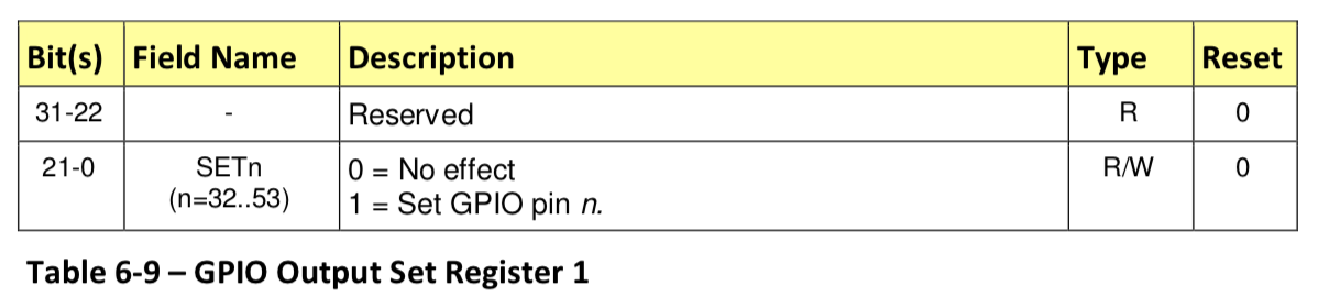
I found this table confusing, because in the prior table, the bit sequence matched the bit ordering. So to keep consistent, the author should have said n=53..32. But, I mapped out what I thought the author meant this way (and turns out I am right):
GPIO 53 52 51 50 49 48 47 46 45 44 43 42 41 40 39 38 37 36 35 34 33 32
bit  21 20 19 18 17 16 15 14 13 12 11 10 9  8  7  6  5  4  3  2  1  0
                        ^
                        |
                        1                   <---
In order to set the GPIO47 pin, we have to shift a 1 15 times into the GPSET1 register (at memory location 0x7E200020). Note that there are two set registers (GPSET0 and GPSET1) to cover all 53 pins. Also note that the set register address is defined back on page 90.
Clearing A GPIO Pin
The procedure for clearing a GPIO pin (setting its potential to 0v) is similar:
The output clear registers are used to clear a GPIO pin. The CLR{n} field defines the respective GPIO pin to clear, writing a “0” to the field has no effect. If the GPIO pin is being used as in input (by default) then the value in the CLR{n} field is ignored. However, if the pin is subsequently defined as an output then the bit will be set according to the last set/clear operation. Separating the set and clear functions removes the need for read-modify-write operations.
Similarly, the clear register definition is:
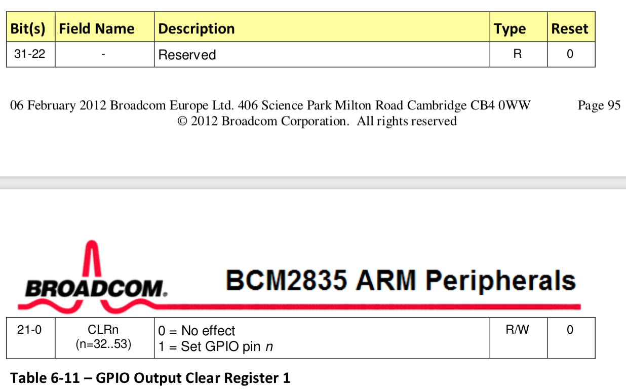
This mirrors the set register definition. To clear the GPIO47 pin, we shift a 1 15 times into the GPCLR1 register (at memory location 0x7E20002C)
Finally! Some Code - How To Code This In Java
Now that we know the “what”, it is time to talk about the “how”. It turns out that the Java part of the exercise is pretty simple. The one difficult bit is setting and retrieving values from registers, because after all, Java does not directly let you access memory. But first, the program:
import haiku.vm.NativeCBody;
import haiku.vm.NativeCFunction;

/**
 * Define access to GPIO registers
 */
@NativeCBody(cImpl ="uint32_t volatile * gpio = (uint32_t volatile *)0x20200000UL;")

/**
 * Make the green ACT LED on the Raspberry Pi Zero blink
 */
public class Main {
  @NativeCFunction(cImpl = "gpio[arg1] = arg2;")
  /**
   * Set the value of a GPIO register.
   * @param registerOffset  The count of the number of registers from
   *                        the beginning offset.
   * @param value           The value to set
   */
  private static native void setGPIO(int registerOffset, int value);

  @NativeCFunction(cImpl = "return gpio[arg1];")
  /**
   * Fetch the value of a GPIO register.
   * @param registerOffset  The count of the number of registers from
   *                        the beginning of the offset.
   * @return                The value of the register fetched.
   */
  private static native int getGPIO(int registerOffset);

  public static final int REG_LEN = 4;                  // Registers are 4 bytes long
  public static final int GPIO_GPFSEL4 = 0x10/REG_LEN;  // GPIO Function Select 4
  public static final int GPIO_GPSET1 = 0x20/REG_LEN;   // GPIO Pin Output Set 1
  public static final int GPIO_GPCLR1 = 0x2C/REG_LEN;   // GPIO Pin Output Clear 1
  public static final int LED_GPF_OUTPUT_BIT = 21;      // GPIO Function Bit For Output, GPIO47
  public static final int LED_GPIO_BIT = 15;            // Set/Clr Bit For GPIO47

  /**
   * Main function entry point for app
   */
  public static void main(String[] args) {
    int tim;

    // Write 1 to the GPIO Function Select field (FSEL47) of the GPFSEL4 register to set
    // the GPIO47 pin for the ACT LED as an output. Don't trounce over data
    // that might already be in the register. This why we are reading the register
    // and then "oring" in the contents to set.
    setGPIO(GPIO_GPFSEL4, (1 << LED_GPF_OUTPUT_BIT) | getGPIO(GPIO_GPFSEL4));

    while(true) {
      // Delay
      for(tim = 0; tim < 50000; tim++);

      // Set the CLR47 field witin the GPCLR1 register, by setting it to 1
      // (thus asserting 0 the GPIO47 pin), which pulls the LED cathode to ground,
      // thus lighting the LED.
      setGPIO(GPIO_GPCLR1, (1 << LED_GPIO_BIT));

      for(tim = 0; tim < 50000; tim++);

      // Set the SET47 field witin the GPSET1 register, by setting it to 1
      // (thus asserting 1 the GPIO47 pin), which pulls the LED cathode to +3.3v.
      // With no voltage drop across the LED, it will not light.
      setGPIO(GPIO_GPSET1, (1 << LED_GPIO_BIT));
    }
  }
}
Referencing the GPIO Base Address
/**
 * Define access to GPIO registers
 */
@NativeCBody(cImpl ="uint32_t volatile * gpio = (uint32_t volatile *)0x20200000UL;")
@NativeCBody is a Java decorator defined within the HaikuVM library which inserts C code into the body of the transpiled Java application, before it is finally compiled into a native image. All of that happens behind the scenes when you build the application. This is how we can directly access memory, by using C! The C code defines a base pointer to a 32-bit integer at the start of the GPIO registers called gpio, starting at address 0x20200000. The reason it is defined volatile is important, but as this blog is already long, you should read How to Use C’s volatile Keyword.
Wait, why not 0x7E200000 per the datasheet, page 90? I’ll get to that in one minute.
Setting A GPIO Register:
  @NativeCFunction(cImpl = "gpio[arg1] = arg2;")
  /**
   * Set the value of a GPIO register.
   * @param registerOffset  The count of the number of registers from
   *                        the beginning offset.
   * @param value           The value to set
   */
  private static native void setGPIO(int registerOffset, int value);
@NativeCFunction is another Java decorator that defines C code within the context of a function, directly mapped to a Java function (the first function below the decorator, setGPIO). The decorator labels arguments from the Java function as argx from left to right within the C code. In this case, the C code uses the gpio pointer as an array accessor to access 32-bit integers starting at the base address, and then replaces whatever the value is at the registerOffset index, known as arg1 within the C function, with the Java value parameter, known as arg2 in C.
Getting GPIO Register Contents:
  @NativeCFunction(cImpl = "return gpio[arg1];")
  /**
   * Fetch the value of a GPIO register.
   * @param registerOffset  The count of the number of registers from
   *                        the beginning of the offset.
   * @return                The value of the register fetched.
   */
  private static native int getGPIO(int registerOffset);
All we do is define another native function accessible from Java that fetches a register value given a 32-bit integer index offset.
Defining Registers And Bit Fields
  public static final int REG_LEN = 4;                  // Registers are 4 bytes long
  public static final int GPIO_GPFSEL4 = 0x10/REG_LEN;  // GPIO Function Select 4
  public static final int GPIO_GPSET1 = 0x20/REG_LEN;   // GPIO Pin Output Set 1
  public static final int GPIO_GPCLR1 = 0x2C/REG_LEN;   // GPIO Pin Output Clear 1
  public static final int LED_GPF_OUTPUT_BIT = 21;      // GPIO Function Bit For Output, GPIO47
  public static final int LED_GPIO_BIT = 15;            // Set/Clr Bit For GPIO47
These values were taken directly from the datasheet discussion above. Note that register definitions are defined as byte offsets from the base address (which match the documentation), and then converted into integer offsets, since that is what the getGPIO and setGPIO functions want. The bit definitions define the number of bits to shift from right to left to set the bit field appropriately.
Setting GPIO47 Pin For Output
    // Write 1 to the GPIO Function Select field (FSEL47) of the GPFSEL4 register to set
    // the GPIO47 pin for the ACT LED as an output. Don't trounce over data
    // that might already be in the register. This why we are reading the register
    // and then "oring" in the contents to set.
    setGPIO(GPIO_GPFSEL4, (1 << LED_GPF_OUTPUT_BIT) | getGPIO(GPIO_GPFSEL4));
We get the register contents of the GPIO function select register 4 GPFSEL4, bit shift a 1 to the 21st bit to form another integer, and then or the two together. In this way, we do not mess with another other data that might be in the register. Also note that pins are by default defined as inputs, which means that bits 22 and 23 must be zeros, which is why I am not messing with them. Then we set the result. GPIO47 is now an output pin.
Turning On The LED
      // Set the CLR47 field witin the GPCLR1 register, by setting it to 1
      // (thus asserting 0 the GPIO47 pin), which pulls the LED cathode to ground,
      // thus lighting the LED.
      setGPIO(GPIO_GPCLR1, (1 << LED_GPIO_BIT));
Here we set the CLR47 bit field within the GPCLR1 register by bit shifting a 1 15 times right to left. This sets GPIO47 to a logic 0, setting the voltage to +0v, putting a net 3.3v potential across the LED, thus lighting it.
Turning Off The LED
      // Set the SET47 field witin the GPSET1 register, by setting it to 1
      // (thus asserting 1 the GPIO47 pin), which pulls the LED cathode to +3.3v.
      // With no voltage drop across the LED, it will not light.
      setGPIO(GPIO_GPSET1, (1 << LED_GPIO_BIT));
Finally we set the SET47 bit field within the GPSET1 register by bit shifting a 1 15 times right to left. This sets GPIO47 to a logic 1, setting the voltage to +3.3v, putting a net 0v potential across the LED, thus turning it off.
Why A GPIO Base Address Of 0x20200000 And Not 0x7E200000?
So I first want to say that the documentation is correct. This gets into needing to read the important parts. In this case, Chapter 1 is VERY important. Being that it is first, I guess that makes sense.
So I suggest you read it now, then come back to this paragraph, because you will probably be confused. I was. The author of this document assumed that you knew some basic BCM2835 architecture concepts. This chip is actually several processing units composed into one physical die. Notably, a OpenGL-ES® 1.1/2.0 VideoCore GPU and an ARM ARM1176JZ-F CPU. These processors share a common peripheral bus. Per the docs:
The peripheral addresses specified in this document are bus addresses. Software directly accessing peripherals must translate these addresses into physical or virtual addresses, as described above.
“As described above” means:
Physical addresses range from 0x20000000 to 0x20FFFFFF for peripherals. The bus addresses for peripherals are set up to map onto the peripheral bus address range starting at 0x7E000000. Thus a peripheral advertised here at bus address 0x7Ennnnnn is available at physical address 0x20nnnnnn.
These address translations are done automatically for you via VC/ARM MMU unit in the Chapter 1 block diagram. And further note that the blocks on the far right of the diagram are for the Linux kernel, which we are not using. So the middle blocks apply to our embedded environment.
-
Embedded Java Hello World On Raspberry Pi Zero and Embedded Java On Raspberry Pi Windows Setup ↩
-
Broadcom and the Raspberry Pi foundation are notorious for errors and omissions in documentation. It is hard to write good documentation, I admit. But still… Just so you are aware, there has been bcm2835 eratta collected. ↩
Spread the Word
If you found this information helpful, I would appreciate a kind mention.
Click to Tweet (you may edit before posting.)
 XRPTipBot tips appreciated too!